


Invisible triumph: how a Finnish invention powers modern microelectronics

Semiconductors are all around us – in computers, smartphones, vehicle control systems, and solar panels. They are materials that conduct electricity better than insulators but worse than metals, with conductivity that can be precisely controlled. The most important semiconductors include silicon, germanium, and certain compounds such as gallium arsenide.
Making semiconductors is an extremely precise, high-tech process that continues to evolve. One of the most important breakthroughs in this field is atomic layer deposition or ALD.
ALD is a thin-film manufacturing method developed in 1974 by Tuomo Suntola, an alum of Aalto University. It can be considered one of Finland’s most important inventions. ALD has long been the fastest-growing production technology in the semiconductor industry. Its primary use is in microelectronics, but it is increasingly applied in batteries, solar cells, and medical coatings. Suntola was awarded the Millennium Technology Prize in 2018 for his invention.
“More and more material layers are being made with ALD. As microelectronics become ever smaller and more efficient, ALD is practically the only option for producing these layers. The smaller the scale we work on, the more essential this technique becomes,” says Professor Ville Miikkulainen from Aalto University’s School of Chemical Engineering.
Despite its importance, the pioneering role of Finland and Tuomo Suntola in ALD is often unknown to the public, perhaps because the technology is hidden inside complex chips and components. Yet ALD is a crucial enabler of modern microelectronics and a vital part of everyday life.
How ALD Works
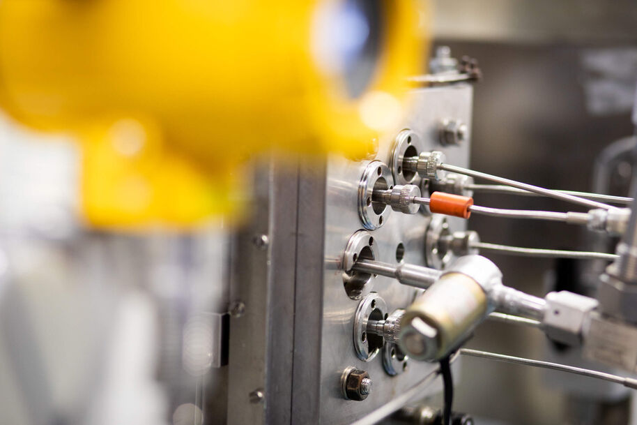
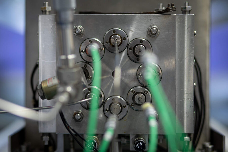
ALD is essential in semiconductor manufacturing because microelectronic components are built layer by layer on a silicon wafer. Each layer affects how the component functions, so it must be uniform and precisely the right thickness.
In the process, source materials are introduced as gases into a reactor. They attach to surfaces through chemical reactions, which stop automatically once the surface is fully covered. The reactor is then flushed, and the next source material is added, reacting only with the newly formed layer. In this way, the film grows one atomic layer at a time in a highly controlled and uniform manner.
“The method is slow but extremely precise. The thickness of the film can be controlled to less than a nanometer, yet it grows uniformly over large, even complex surfaces,” Miikkulainen explains.
Towards more efficient and eco-friendly processes
Miikkulainen’s research group focuses on improving ALD processes and understanding their chemical reactions—essential for producing energy materials needed for the green transition. For example, ALD coatings on electrodes can significantly enhance the lifespan and performance of lithium-ion batteries.
“For many important materials, ALD processes do not yet exist, and existing ones need improvement. That is what makes this research exciting—there is potential not just in microelectronics, but in many emerging fields,” Miikkulainen says.
Researchers are also developing new ALD applications, such as photocatalysts, which accelerate chemical reactions using light without being consumed. Light-assisted ALD processes are under development, where light triggers the surface reaction, allowing precise patterns on thin-film layers by controlling where the film grows.
“Precise patterning of thin films is essential in microelectronics. Current lithography methods are complex, expensive, and wasteful. By directing ALD growth with light, we can ‘write’ thin-film patterns directly on surfaces, simplifying the process and reducing waste. However, light-assisted ALD is still limited and not yet ready for complex microelectronic structures,” Miikkulainen explains.
Ville MiikkulainenAs microelectronics become smaller and more efficient, ALD technology becomes increasingly essential.
ALD/MLD hybrid technique expands applications
In addition to ALD, researchers at Aalto University are exploring molecular layer deposition (MLD). MLD allows the creation of hybrid thin films that combine organic and inorganic layers. Using the ALD/MLD hybrid technique, traditional inorganic films can be made flexible, less thermally conductive, or optimized for light absorption. These films are being developed for micro-batteries, solar cells, and thermoelectric devices.
Professor Maarit Karppinen has been a key figure in combining ALD and MLD. Her team has developed processes that alternate inorganic and organic layers one atomic or molecular layer at a time, enabling precise control over hybrid materials.
“Our goal is to develop entirely new materials – ones that cannot be made by any other method. Designed at atomic and molecular precision, these materials can open entirely new possibilities,” Karppinen says.
“For example, mechanically reinforced films. By adding organic layers to inorganic films using MLD, they become flexible and suitable for wearable electronics – something ALD alone cannot achieve,” she adds.
Karppinen’s team is also developing materials for new energy storage and conversion technologies, such as cobalt-free organic battery electrodes and solar-cell materials that absorb light over a broader wavelength range.
Finland and Aalto at the global forefront
For a country of its size, Finland is exceptionally strong in ALD, with researchers at Aalto University and the University of Helsinki recognized as international leaders.
“The international ALD conference was held in Helsinki last year, 50 years after the first ALD patent. This shows Finland’s prominent position in the field. We have a long history and strong research groups and companies that have remained here thanks to our expertise,” Miikkulainen says.
Finnish companies such as Picosun and Beneq manufacture ALD equipment, with offices at Aalto’s Micronova building. They are continuously exploring applications beyond microelectronics. Picosun is now part of Applied Materials, where Finnish expertise remains highly valued. Karppinen’s group collaborates with the company on projects in semiconductors and sustainable process development.
The future of semiconductor research in Finland and at Aalto is bright. The field is rapidly evolving, and research here continues to provide a foundation for innovation.
“Aalto-trained students and doctoral graduates have found employment both in Finland and abroad, and their expertise is highly valued. There is clearly strong interest in this field among students,” Karppinen says.

Aalto University
Aalto University
Donate and join Aalto in becoming a global leader in sustainable innovation.
Read more news

Bachelor's Students Successfully Complete Research Internship
Three bachelor's students have successfully completed their research internships.
From Materials to Smart Textiles: Benjamin Begins a New Chapter at Aalto
Ping-Chun Chen is a researcher from National Tsing Hua University, Taiwan.
The idea of three researchers generated a deep tech company
Sim Analytics Oy relies on strong research expertise. Its story began when three researcher colleagues working in different laboratories at LUT University began to consider how to provide and analyse data in a way that would support industrial companies in making business decisions.