In-Situ TEM

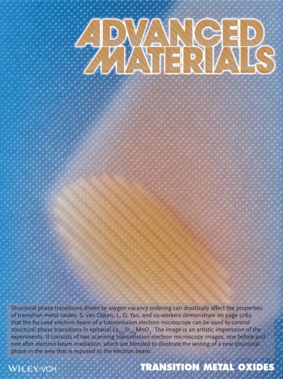
The commercialization of aberration-corrected TEMs is one of the most exciting developments in nanomaterials characterization. Together with the integration of energy dispersive X-ray spectroscopy (EDS) and electron energy loss spectroscopy (EELS), the structural and elemental composition of nanomaterials can now be determined with atomic resolution. Additionally, it is possible to manipulate materials actively inside a TEM using special sample holders for heating, cooling, electrical biasing, and mechanical nanoprobing. Recently, we have developed a platform for in-situ TEM measurements at the OtaNano Nanomicroscopy Center of Aalto University. Our investigations focus on high-resolution imaging of structural, chemical, and resistive phase transitions that are driven by oxygen vacancy migration. For instance, we demonstrated that electron-beam irradiation of an epitaxial La2/3Sr1/3MnO3 film changes its as-grown perovskite structure into an oxygen-deficient brownmillerite phase [1]. Using a nanoprobing holder, we directly imaged oxygen vacancy-driven structural and resistive phase transitions in La2/3Sr1/3MnO3 films during voltage pulsing [4]. In another study, we showed that oxygen vacancy ordering into 2D or entirely new 3D patterns can be attained in La0.5Sr0.5CoO3-d films through thermal cycling [6] or in La2/3Sr1/3MnO3–δ film films by mechanical nanoprobing [7].

We also use our in-situ TEM measurement platform for high-resolution structural characterization of various other nanomaterials. For instance, we monitored the migration of oxygen vacancies under applied bias voltages in a magneto-ionic Pt/Co/GdOx structure using high-resolution STEM-EELS [2]. In this study, the in-situ STEM-EELS experiments were combined with ex-situ magnetic measurements of voltage-controlled magnetism. To understand the origin of giant resistive switching in ferroelectric tunnel junctions, we characterized the termination and roughness of BaTiO3 , PbTiO3, or PbZrxTi1−xO3 tunnel barriers. We also used in-situ TEM to characterize unconventional ferroelectric switching via local domain wall motion in multiferroic epsilon-Fe2O3 films [5]. Our measurements showed that ferroelectric switching at moderate electric fields in this material occurs around pre-existing domain walls only.
Publications
1. L. Yao, S. Majumdar, L. Äkäslompolo, S. Inkinen, Q. Qin, S. van Dijken. Electron-beam-induced perovskite-brownmillerite-perovskite structural phase transitions in epitaxial La2/3Sr1/3MnO3 films. Advanced Materials 26, 2789 (2014).
2. U. Bauer, L. Yao, A.J. Tan, P. Agrawal, S. Emori, H.L. Tuller, S. van Dijken, G.S.D. Beach. Magneto-ionic control of interfacial magnetism. Nature Materials 14, 174 (2015).
3. Q.H. Qin, L. Äkäslompolo, N. Tuomisto, L. Yao, S. Majumdar, J. Vijayakumar, A. Casiraghi, S. Inkinen, B. Chen, A. Zugarramurdi, M. Puska, S. van Dijken. Resistive switching in all-oxide ferroelectric tunnel junctions with ionic interfaces. Advanced Materials 28, 6852 (2016).
4. L. Yao, S. Inkinen, S. van Dijken. Direct observation of oxygen vacancy-driven structural and resistive phase transitions in La2/3Sr1/3MnO3. Nature Communications 8, 14544 (2017).
5. X.X. Guan, L.D. Yao, K.Z. Rushchanskii, S. Inkinen, R.C. Yu, M. Lezaic, F. Sanchez, M. Gich, S. van Dijken. Unconventional ferroelectric switching via local domain wall motion in multiferroic epsilon-Fe2O3 films. Advanced Electronic Materials 6, 1901134 (2020).
6. S. Inkinen, L.D. Yao, S. van Dijken. Reversible thermal strain control of oxygen vacancy ordering in an epitaxial La0.5Sr0.5CoO3-d film. Physical Review Materials 4, 046002 (2020).
7. L.D. Yao, S. Inkinen, H.P. Komsa, S. van Dijken. Structural phase transitions to 2D and 3D oxygen vacancy patterns in a perovskite film induced by electrical and mechanical nanoprobing. Small 17, 2006273 (2021).


