


ATMOC (2021-2024)
Designing efficient optical and optoelectronic products requires nanomaterials with specific properties and dimensions. In the optics and semiconductor industry, the characterization of suitable nanomaterials is a challenging task. It may require accurate data acquisition, modelling, and reliable uncertainty estimation.
The purpose of this project was to create a framework for measuring the optical properties of thin-film structures over a wide range of wavelengths from infrared to X-rays. The practical characterization methods comprised traceable reflectometry, Mueller ellipsometry, and scatterometry techniques. Inverse modelling and virtual measurement methods were also advanced in this project.
The role of the Metrology Research Institute (MRI) of Aalto University in this project was to contribute to the spectrophotometric measurements and analysis of thin film and test materials using Aalto’s gonioreflectometry and spectrophotometry facilities. Furthermore, MRI used mathematical modelling to determine the optical constants and thickness of components of single-layer thin film structures and multilayer complex nanostructures.
Single-layer structure analysis included pre-characterization of twelve SiO2 and two Al2O3 thin film samples on Si substrates. The measurements were performed using the Sentech micro-reflectometer with a 100-micrometer beam size (shown in Figure 1).
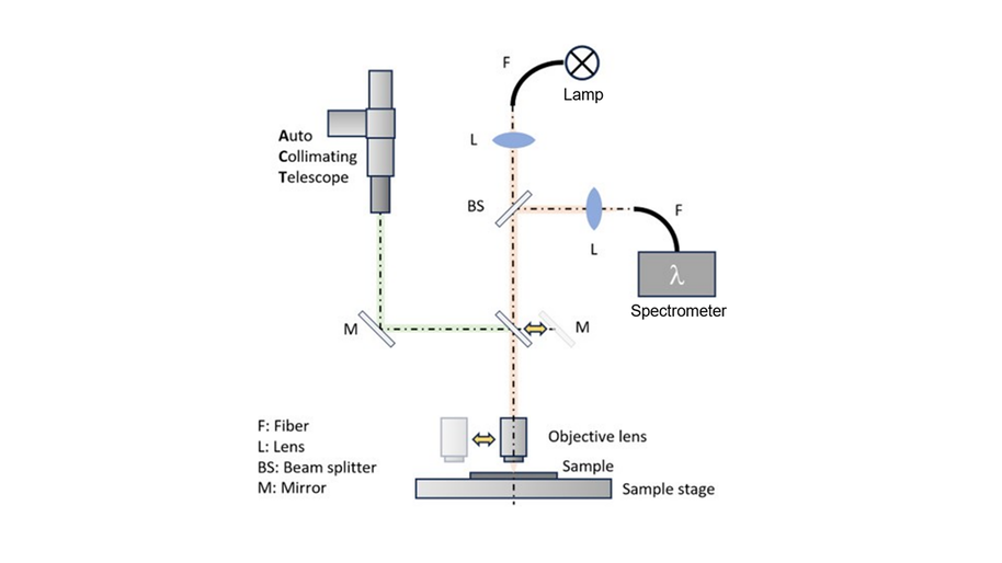
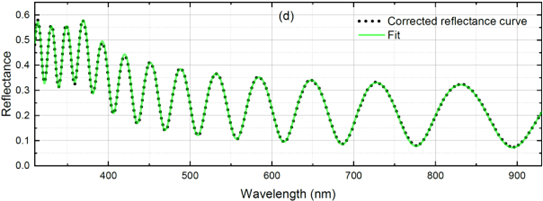
The micro-reflectometer operated in the spectral range of 310 to 930 nm. We used a dedicated software which utilizes transfer matrix method (TMM) to fit the measured reflectance to obtain the thickness of the samples. Based on the geometry of microscope-based reflectometers, we developed a method to consider the distribution of the incident angles within a cone, the bandwidth effect and possible thickness variations in the samples. Using this method is crucial to improve our fitting process especially for the samples with thicker layers. Figure 2 shows the improved fit for the 2 µm SiO2 on Si sample [1].
Multilayer complex nanostructures, where one of the thin layers consists of vacuum or air, are called PillarHalls. It has been developed to test new conformal thin film materials (Figure 3).

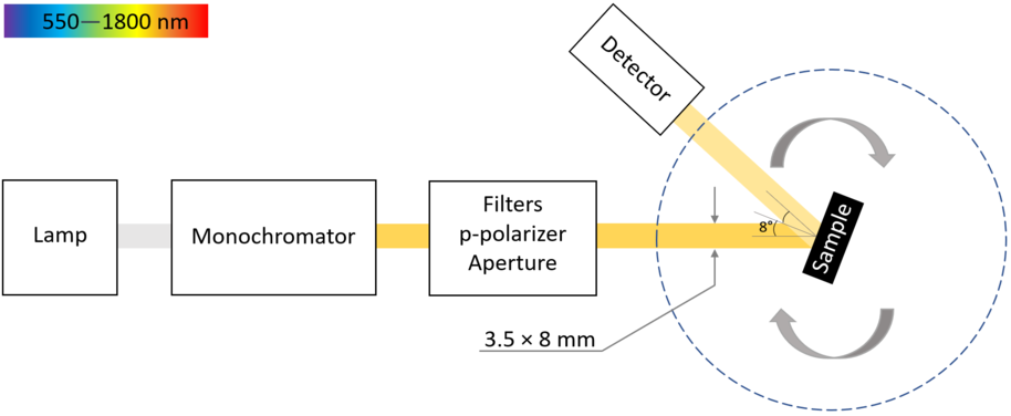
The PillarHall sample, featuring a nominal air gap height of 100 nm, was subjected to reflectometry measurements using a Cary 7000 spectrometer within a wavelength range 550-1800 nm (Figure 4).
Then this measurement data were analyzed with dedicated MATLAB code. The fitted reflectance spectrum for the three-layer model, as depicted in Figure 5, revealed an air gap thickness of 86 nm. The PolySi layer has a rectangular distribution of thickness values between 1590 nm and 1610 nm within the beam size [2].
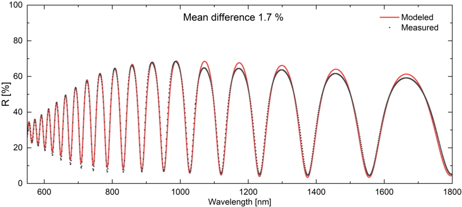
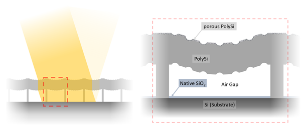
In the next step, we developed a more advanced model for the PillarHall sample with a nominal air gap height of 500 nm, taking into account the periodic porosity of the top layer as well as the bending of the PolySi layer [3]. Figure 6 illustrates the bending model used for the optical characterization.
The fitting results shown in Figure 7 indicate a clear improvement in the agreement between the measured and modelled curves, leading to a more reliable and accurate characterization of the air-gap thickness variation. Using the advanced model, the air gap height for this sample was determined to be 460 nm. For comparison, applying a simpler model that neglects both bending and indentations yields an air-gap value of 464 nm. These results demonstrate that reflectometry measurements in the visible and infrared wavelength range provide sufficient information for analyzing such thin-film structures, enabling reliable estimation of layer thicknesses.

[1] Masoud Rastgou, Aleksandr Danilenko, Farshid Manoocheri, Erkki Ikonen, "Optimizing measurement accuracy in microscope-based reflectometry for thin film optical properties." Measurement Science and Technology 36, 075001 (2025). https://doi.org/10.1088/1361-6501/ade329
[2] Aleksandr Danilenko, Masoud Rastgou, Farshid Manoocheri, Jussi Kinnunen, Virpi Korpelainen, Antti Lassila, Erkki Ikonen, "Characterization of PillarHall test chip structures using reflectometry technique." Measurement Science and Technology 34, 096006 (2023). https://doi.org/10.1088/1361-6501/acda54
[3] Aleksandr Danilenko, Masoud Rastgou, Farshid Manoocheri, Jussi Kinnunen, Virpi Korpelainen, Antti Lassila, Erkki Ikonen, "Reflectometry technique