News

Exploring the nanoscale world

Are you curious about what happens in Micronova, the leading micro and nanotechnology research center of Finland? This fall we followed students getting hands on experience in the most common methods used in micro and nanotechnology on the Micronova Laboratory course.
Aalto University / students using a microscope in the Micronova cleanroom / photo: Linda Koskinen
The Micronova Laboratory course consists of five guided laboratory sessions. Photo: Linda Koskinen

Monday 14.10.2019

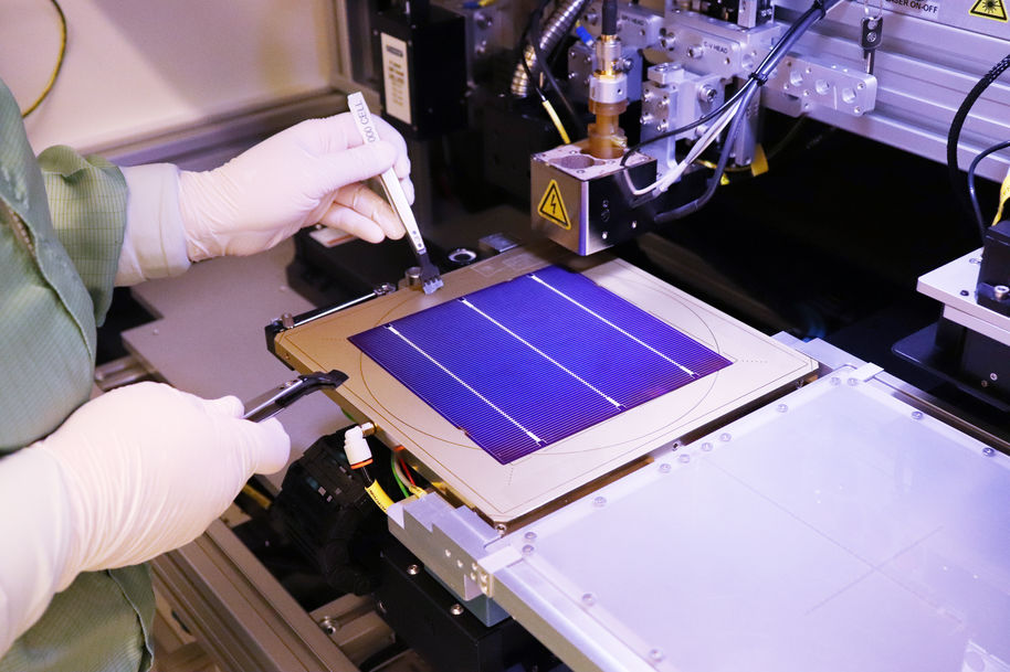
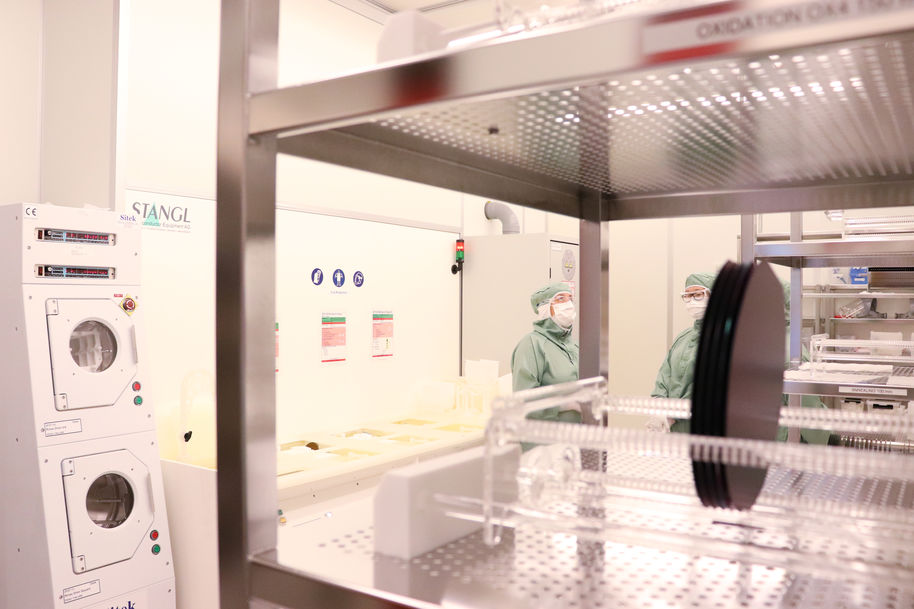
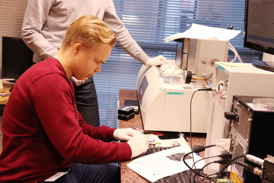
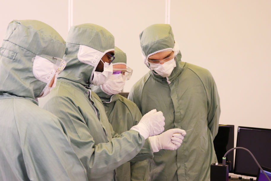
How does a solar cell work and what are the problems you need to take care of in order to get a solar cell work efficiently? This was the topic of the very first lab session of the Micronova Laboratory course. The students studied a wafer and a finished cell and were given the task to figure out what had caused the differences between the two. Hints for this puzzle were given on a cleanroom tour on which methods and equipment used in the process of making solar cells were presented.

Aalto University / Students watching a solar cell in the Micronova cleanroom / photo: Linda Koskinen
The topic of the first laboratory session was solar cells.
Aalto University / A solar cell / photo: Linda Koskinen
A finished solar cell.
Aalto University / wafers in the Micronova cleanroom / photo: Linda Koskinen
The students got a cleanroom tour on which methods and equipment used in the process of making solar cells were presented.

Monday 21.10.2019

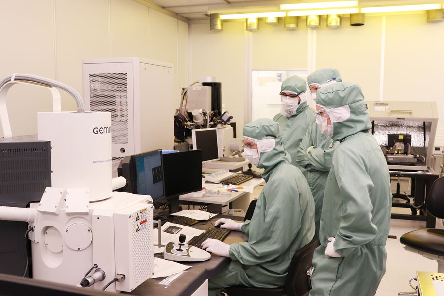
“Now that's cool!" On the second lab session students were given an introduction to the scanning electron microscope. They got hands-on practice with the tool by imaging a sample of compound semiconductor nanowires. These crystalline structures typically have the length of some tens of micrometers – that's one millionth of a metre – so they are tiny! Due to their useful optical, electrical, and mechanical properties they have a vast range of applications in several fields including photovoltaics, optoelectronics, photonics, and electronics.

Aalto University / scanning electron microscope in the Micronova cleanroom / photo: Linda Koskinen
The students were given an introduction to the scanning electron microscope.
Aalto University / students using a scanning electron microscope / photo: Linda Koskinen
The reason behind the overalls is this: the technology developed in the Micronova cleanroom is so minuscule that even a single dust particle can break it – not to mention a single hair!

Friday 8.11.2019

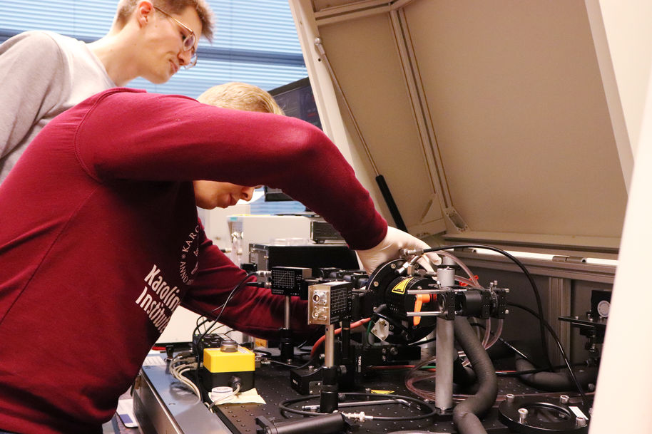
The third lab session was about thermal conductivity. By engineering the thermal properties in nanomaterials used in modern micro- and nanoelectronics, it’s possible to achieve big improvements in power consumption and energy efficiency in, for example, mobile phones. The students familiarised themselves with the effects of nanostructuring on material thermal properties and got to use an optical pump-probe thermoreflectance setup.

Aalto University / Micronova Laboratory course session / photo: Linda Koskinen
The third lab session was about thermal conductivity.
Aalto University / an optical pump-probe thermoreflectance setup / photo: Linda Koskinen
The students got a chance to use an optical pump-probe thermoreflectance setup.

Thursday 21.11.2019

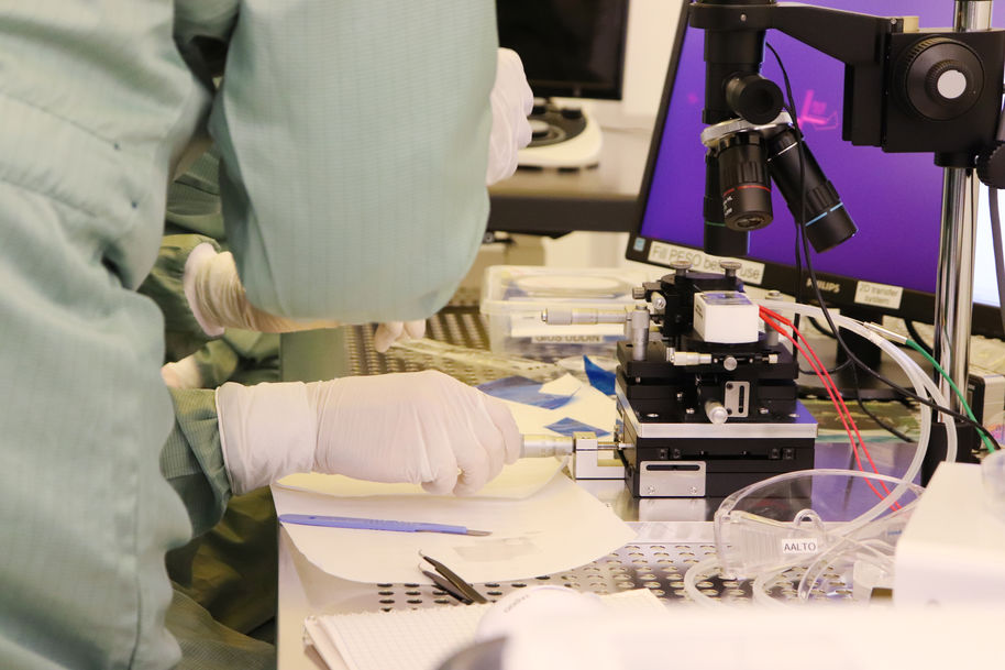
Photonics – the science of light – was the topic of the fourth lab session. The students got to try a method called ‘dry-transfer’: they obtained atomically thin flakes of a two-dimensional material called molybdenum disulfide and transferred a flake onto a silicon chip to make devices like transistors out of it. 2D layered materials have unique mechanical and optoelectronic properties that can be combined in a single device such as flexible displays.

Aalto University / students learning about dry-transfer / photo: Linda Koskinen
The students got to try a method called ‘dry-transfer’.
Aalto University / A Micronova laboratory course session / photo: Linda Koskinen
A thin flake of molybdenum disulfide was transferred onto a silicon chip.

Thursday 12.12.2019

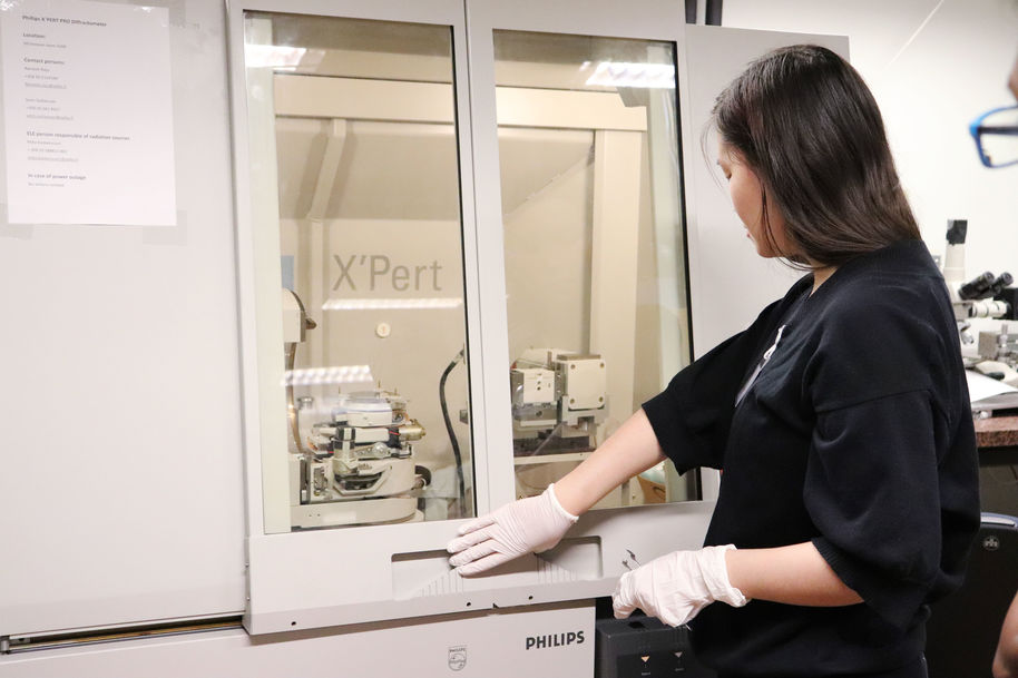
A human hair is about 50 000 nanometers thick. But how can you determine the thickness of a 10–1000 nanometer thin film? On the last lab session students learned about X-ray reflectometry – an analytical technique for investigating thin-layered structures, surfaces and interfaces using the effect of total external reflection of X-rays. First, a hafnium oxide coating was grown on a silicon substrate thin film using atomic layer deposition. As the density difference of the thin film and the substrate causes interference in the low angle X-ray reflection, the students were able to determine the film’s thickness, density and roughness.

Aalto University / Students explaining X-ray reflectometry using pens / photo: Linda Koskinen
The students used pens to explain X-ray reflectometry.
Aalto University / A student on the Micronova Laboratory Course / photo: Linda Koskinen
Thin film’s thickness was determined using X-ray reflectometry.

Got interested?

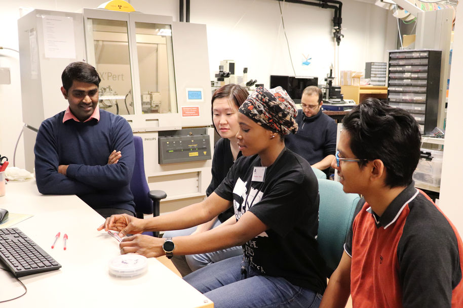
The Micronova Laboratory course is part of the Master's Programme in Electronics and Nanotechnology.

Aalto electronics-ICT anechoic chamber for 2-60 GHz and two near-field scanners

Electronics and Nanotechnology, Master of Science (Technology)

By developing modern hardware technology, electronics and nanotechnology experts play a key role in shaping the future.

Study options
  • Published:
  • Updated:

Read more news

Three female students studying
Research & Art Published:

Seed funding available to boost collaboration between Aalto, KU Leuven and University of Helsinki

Aalto University, KU Leuven and the University of Helsinki launch the 2nd exploratory seed funding call to explore research collaboration possibilities. The funding call is open until 10 September 2024.
Aalto-wide sustainability minor logo
Studies Published:

Aalto’s New Cross-Cutting Minor: Luonnonvarojen kestävä käyttö

Aalto’s new multidisciplinary minor, Luonnonvarojen kestävä käyttö is ready to add to your study plan!
Woman reading using tablet
Studies Published:

Aalto EE Introduces Alex: A New Learning Experience Platform to Transform Lifewide Learning and Tackle Upskilling Challenges

Aalto University Executive Education (Aalto EE) is launching the first version of Alex in June, a learning platform designed to enhance continuous professional development. Alex offers personalized learning journeys, micro-credentials, and professional development programs, aligning current skills with industry needs. This platform, which continuously evolves with new features like mobile access and AI integration, sets a new standard for professional development in Finland.
Nine large blocks of ice formed an art installation at Kansalaistori square in Helsinki 2021
Cooperation, Research & Art, Studies, University Published:

Aalto ARTS Summer School explores the significance of water through the lens of art

The theme of School of Arts, Design and Architecture’s Summer School this year is water, and its significance is explored in a multidisciplinary way through the perspectives of art, film and digital.